


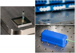
Coupling and Packaging
In addition to supplying enabling optical I/O (input/output) components (PROFA1D, PROFA2D) to you or your preferred packaging vendor for wafer-level probing, coupling or packaging, Chiral Photonics also offers optoelectronic packaging services.
We offer coupling and packaging services that can include both electrical and optical I/O. Send us your diced chips and we will return packaged and connectorized devices with fast turnaround. Alternately, we can help you develop a process and work with you to transfer it fully to you. We aim to work with our customers in the best way suited to their needs. Speak to us early in your design process to discuss your needs with regard to:
- Low-loss edge or face coupling, using a growing array of coupler options, for both probing and packaging.
- Packages customized to application needs for high frequency, low frequency or all-optical/passive applications and optimized to meet your form factor requirements.
- Pigtailed or pluggable package designs.
- Device operating conditions and package/test requirements: cryogenic, high temperature, hermetic.
In order to assist customers in planning for optical packaging, we offer a free Optical Coupling & Packaging Design Guide. We encourage consideration of the packaging design early in the process to avoid common mistakes that could complicate the packaging process.
Contact us to obtain a copy of our free coupling and packaging design guidelines: Contact Us
Exemplary Coupling and Packaging
Below are a sampling of exemplary coupling/packaging jobs that we have done that have been published. Our solutions and experience continue to expand with our customers’ needs across a broad variety of wavelength, bandwidth, package-type and application needs:
High Density Optical Packaging of High Radix Silicon Photonic Switches
- 61-channel flexible tip PROFA2D surface coupled to high radix (64 x 64) silicon photonic MEMS switch.
- 61-channel I/O is accomplished in single port and one alignment step.
- I/O occupies a compact space of 330 μm x 280 μm – more than 200 times smaller than a comparable linear fiber array with 127 μm standard pitch.
T. J. Seok, V. I. Kopp, D. Neugroschl, J. Henriksson, J. Luo, and M. C. Wu, “High Density Optical Packaging of High Radix Silicon Photonic Switches,” in Optical Fiber Communication Conference Postdeadline Papers, OSA Technical Digest (online) (Optical Society of America, 2017), paper Th5D.7.

Silicon Photonics Arrayed I/O
37-channel, single port coupling to 10 μm MFD vertical grating couplers developed for IMEC:
- Single-port, 37-channel, 40 µm channel pitch, SM surface coupling using
- < 3 dB coupling loss (1 dB on top of VGC coupling loss)
P. De Heyn, et. al., “Ultra-Dense 16x56Gb/s NRZ GeSi EAM-PD Arrays Coupled to Multicore Fiber for Short-Reach 896Gb/s Optical Links,” in Optical Fiber Communication Conference, OSA Technical Digest (online) (Optical Society of America, 2017), paper Th1B.7.
V. I. Kopp, et. al., “Two-dimensional, 37-channel, High-bandwidth Ultra-dense Silicon Photonics Optical Interface,” in Optical Fiber Communication Conference: Postdeadline Papers, (Optical Society of America, 2014), paper Th5C.4

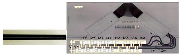
Silicon Photonics Arrayed I/O
10-channel coupler, developed for IBM:
- Single-port, 10-channel, 20 µm channel pitch, linear array, PM edge coupling to 2 μm MFD waveguides
- Channel crosstalk below -35 dB
- 8-Tb/s/mm bandwidth densities using only four wavelengths
F. E. Doany, et. al., “Multichannel High-Bandwidth Coupling of Ultradense Silicon Photonic Waveguide Array to Standard-Pitch Fiber Array,” Lightwave Technology, Journal of , vol.29, no.4, pp.475, Feb.15, 2011.
B. G. Lee et al., “20-μm-pitch eight-channel monolithic fiber array coupling 160 Gb/s/channel to silicon nanophotonic chip,” 2010 Conference on Optical Fiber Communication (OFC/NFOEC), collocated National Fiber Optic Engineers Conference, San Diego, CA, 2010, pp. 1-3.
InP Coherent Receiver Arrayed I/O
Two-channel coupler, developed for Bell Laboratories, Alcatel-Lucent:
- Single-port, 2-channel, 19 µm channel pitch, PM coupling to 2 μm MFD waveguides
- < 2 dB coupling loss (fiber-to-chip)
C. R. Doerr, L. Zhang, and P. J. Winzer, “Monolithic InP Multi-Wavelength Coherent Receiver,” in Optical Fiber Communication Conference, OSA Technical Digest (CD) (Optical Society of America, 2010), paper PDPB1

Silicon Photonics Hermetic Butterfly Package
- Single-port, single-channel, PM edge coupling to 2 μm MFD waveguide
- FTNIR spectrometer for oil and gas sensing application
Development Package
Open design, optically-coupled package enabling electronic probing, developed for OpSIS:
Dual port, single channel optical edge coupling using PROFA1D
- 1550 nm PANDA fiber coupled to 220 x 200 nm Si waveguide
- < 2 dB coupling loss (fiber-to-chip)
- < -20 dB polarization crosstalk
- Designed for thermal stability and cryogenic testing


Contact us to discuss your design process and packaging needs Contact Us